Product outline
SF160ACT is a high-resolution micro-focus X-ray system for the inspection of semiconductor, PCB assembly, and electronic component. With its superior X-ray imaging, micro-scale hidden defects can be detected in high resolution.
SF160ACT equips 160kV micro-focus open tube with 1um spot size. The system can magnify the object up to 4,800x and display the X-ray image at any angle using 6-axis manipulator configuration.
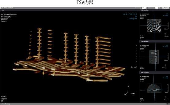
3D CT(Computed Tomography) visualizes all hidden structure and even micro-scale defects inside the object. SEC unique oblique CT technology realizes high-magnified 3D CT visualization of large sample. Generally, it is known that CT scanning is limited by the object size, but oblique CT technology overcomes the size limitation and can be adapted to PCB assemblies, large-size Multilayer boards and even to semiconductor wafers.
Major Features
- 1・ Spot Size
- 160kV Micro-focus X-ray Open Tube
- Flat Panel X-ray Detector
- Table Size: 510mm x 460mm
- 7-axis (X, Y, Z, R, T, Y-aft, CR-R) of configuration
- Customer oriented GUI and Variable functions
- Dual CT System (Cone Beam & Oblique CT)
Application Examples
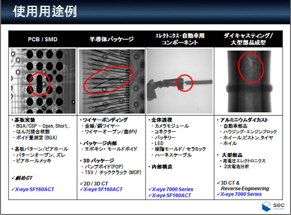
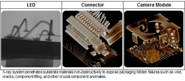
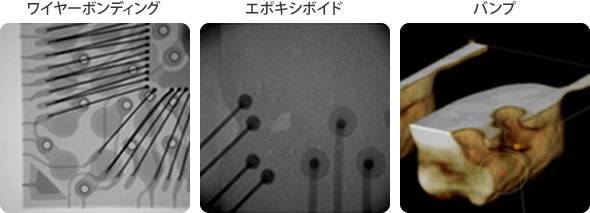
Semiconductor Packaging / LED
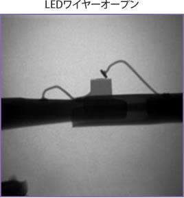
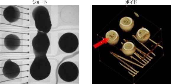
| Wire Bonding | Wire short, Wire open, Sweeping |
|---|---|
| Bump | Pattern flaking, Void, Crack |
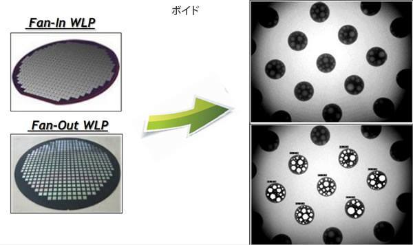
| 3D packaging | MCP, TSV, FCB Micro defect |
BGA/CSP
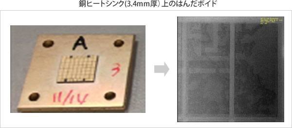
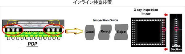
| BGA/CSP | Open, Crack, HIP, Cold Solder | General Solder Bonding such as Bridging, Void | AXI of BGA Voids |
|---|
Electronic Components
| Connector | Internal wire bonding |
|---|---|
| Camera module | Components bonding |
| eneral patter Open / Short | Micro contamination |